


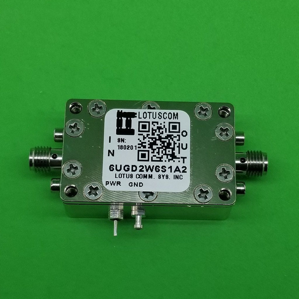


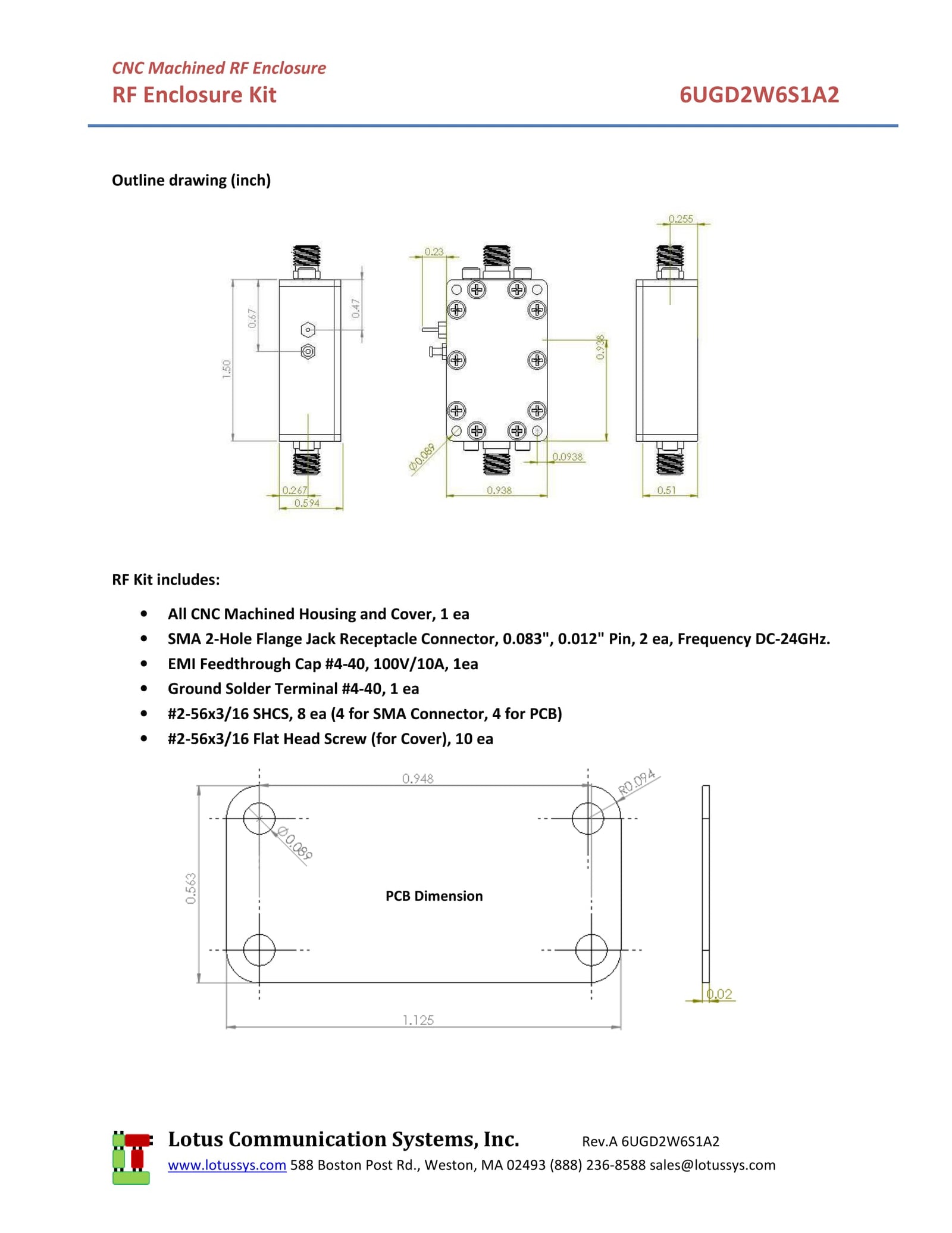

6UGD2W6S1A2 Enclosure Kit for 0.020"/0.5mm PCB (size 1.125"x0.5625") 2 SMA Active 0.58" Height
$ 176.00 USD
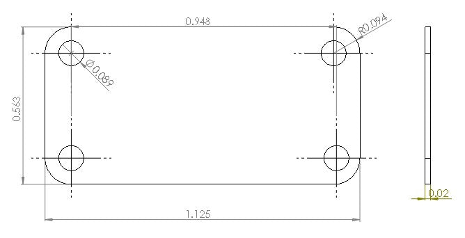
Part Number: 6UGD2W6S1A2 is RF Designer Kit for RF prototyping with PCB size of 1-1/8"x9/16"x0.020"(or 0.5mm).
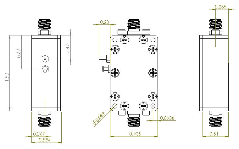
RF Housing Size: 8Ux5U (1-1/2"x15/16"). Each U is 3/16". Housing height: 0.58". The PCB mounting hole spacing is 0.9375" and 0.375" respectively. PCB Inside Clearance to Enclosure Cover is 0.26". The EMI Feedthrough for Power is on the center of PCB with pin size 0.032". This Enclosure is ideal to hold Active PCB circuit (e.g., LNA, Frequency Conversion Circuits etc.).
Proudly Made in USA by Lotus Communication Systems, INC. in Massachusetts.
RF Kit include (PCB is not included):
- All CNC Machined Housing and Cover, 1 ea
- SMA 2-Hole Flange Jack Receptacle Connector, 0.083", 0.012" Pin, 2 ea
- EMI Feedthrough Cap #4-40, 100V/10A, 1ea
- Ground Solder Terminal #4-40, 1 ea
- 2-56x3/16 SHCS, 4 for SMA Connector
- 2-56x5/32 SHCS, 4 for PCB
- 2-56x3/16 Flat Head Screw (for Cover), 8 ea
Features
- Hold PCB Size 1-1/8"x9/16"x0.020" (or 0.5mm)
- All CNC Machined Surface for Superior Finish and Minimize RF Leakage
- 4 Installation Holes to Mount Kit to Back Board with #2 SHCS
- 3/16" Wall Thickness for Strong Mechanical Strength
- Two SMA Connector
- Electroless Nickel Plating per MIL-C-26074, ASTMB 733
- Professional Zebra Ultimate Label for Outdoor Usage
- Proudly MADE IN USA (Material & Labor)
- ROHS Compliant
Applications
- Cell
- Microwave Radio
- Test Instrumentation
- SDR & Ham Radio
Resources